Lab 6 - ECE 421L
Email Address: cortej2@unlv.nevada.edu
Lab Date: Oct 9,2019-Oct 16,2019
------------------------------------------------------------------------------------------------------------------------------------------------------------------------------------------------------------------------------------------
Prelab:
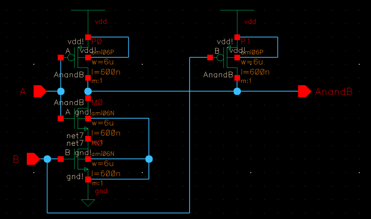
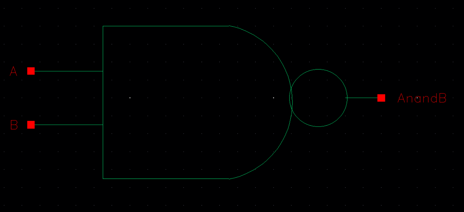
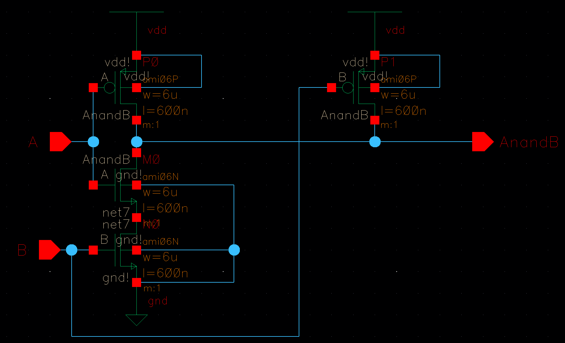
I created the schematic and symbol for a NAND gate with two inputs and one output as seen below.
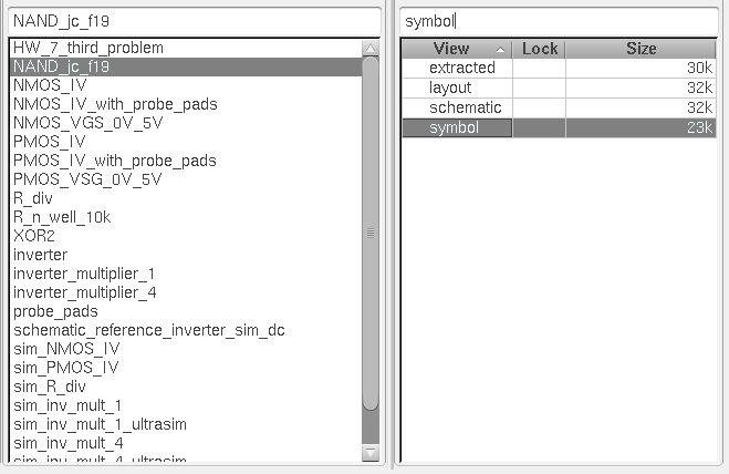
| NAND2 schematic | NAND2 symbol |
| |
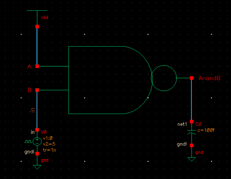
I then created a duplicate nand2 schematic set up to simulate the nand2.
| NAND2 simulation schematic | NAND2 simulation results |
 | 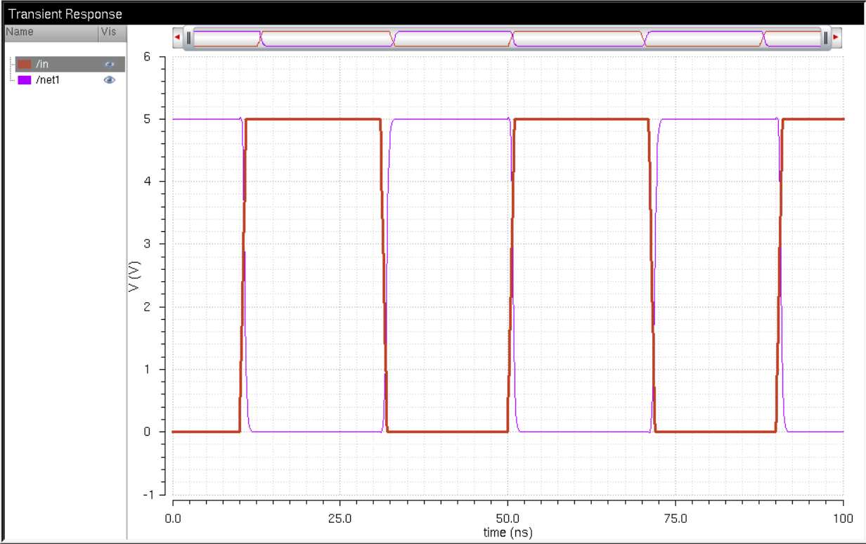 |
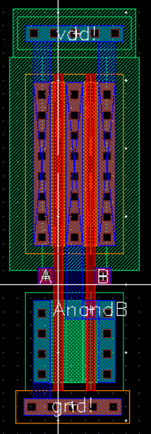
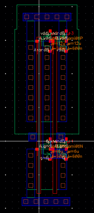
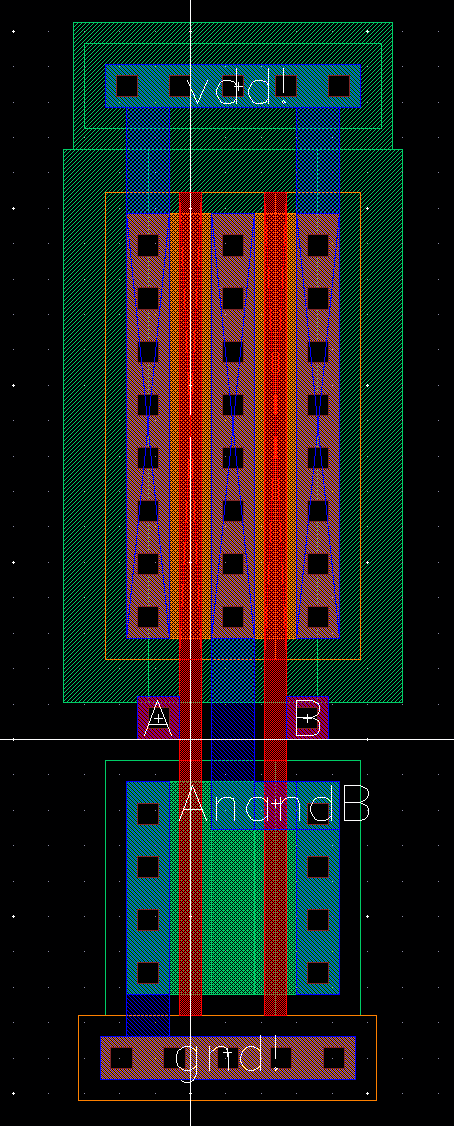
I then created the layout for nand2.
| NAND2 layout | NAND2 extracted |
 |  |
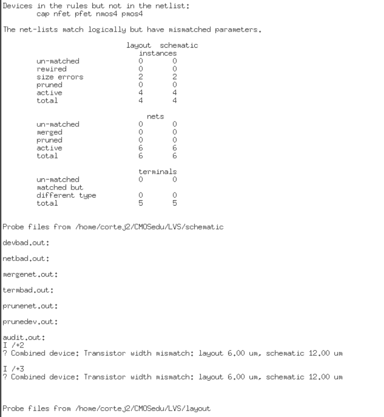
Tutorial 4 (prelab 6) ended with some LVS errors which are shown below.
| NAND2 LVS |
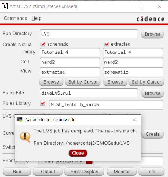 |
| LVS error message |
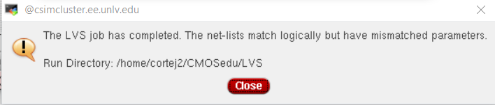 |
| LVS error message in detail |
 |
------------------------------------------------------------------------------------------------------------------------------------------------------------------------------------------------------------------------------------------
Lab:1) Creating NAND and XOR gates
I created the schematic, layout and symbol for a two input NAND and a two input XOR gate.
Below is the cell name, schematic, layout, DRC symbol and LVS for the NAND gate.
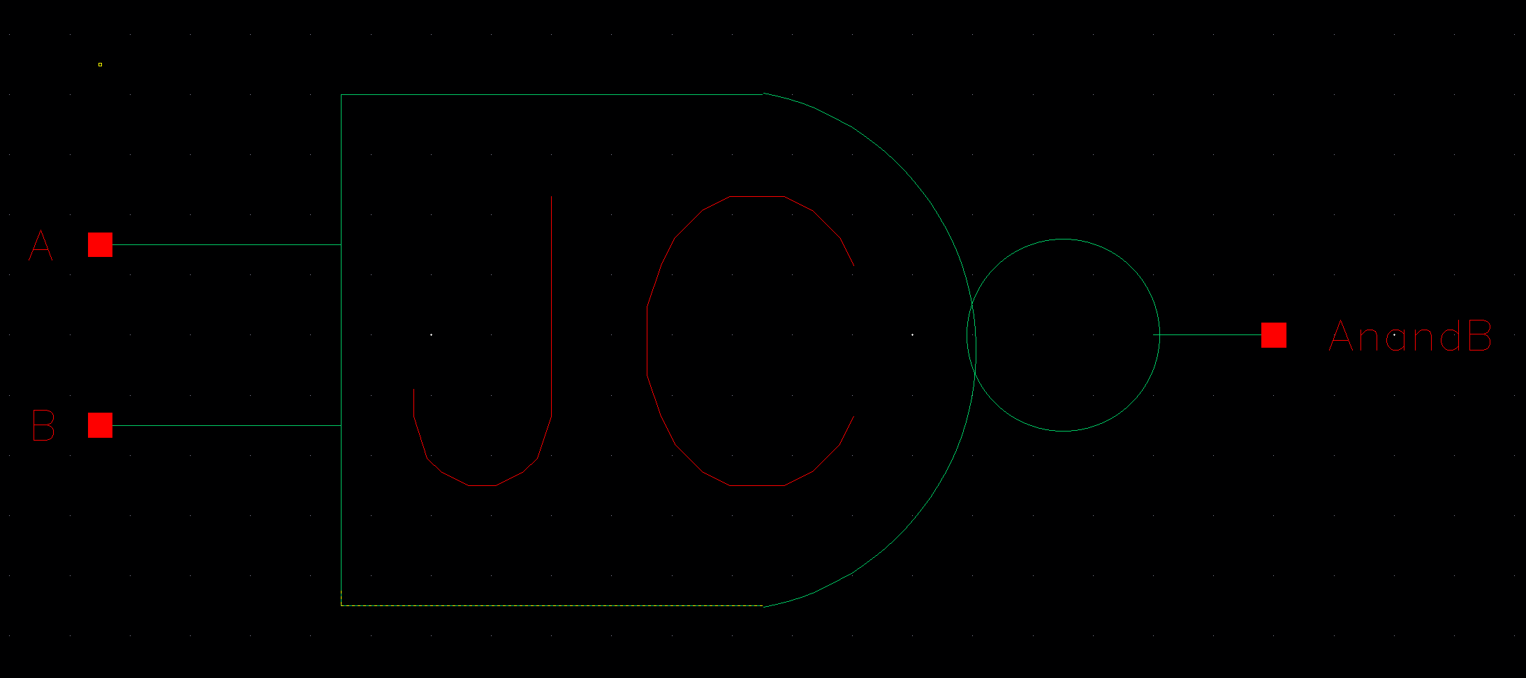
| NAND cell name | NAND schematic |
 |  |
| NAND layout | NAND symbol |
 |  |
| NAND DRC | NAND LVS |
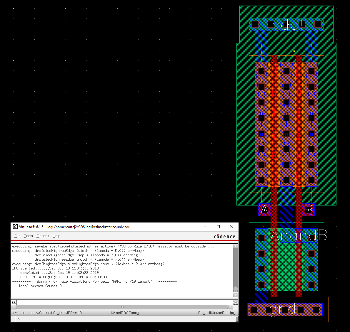 | 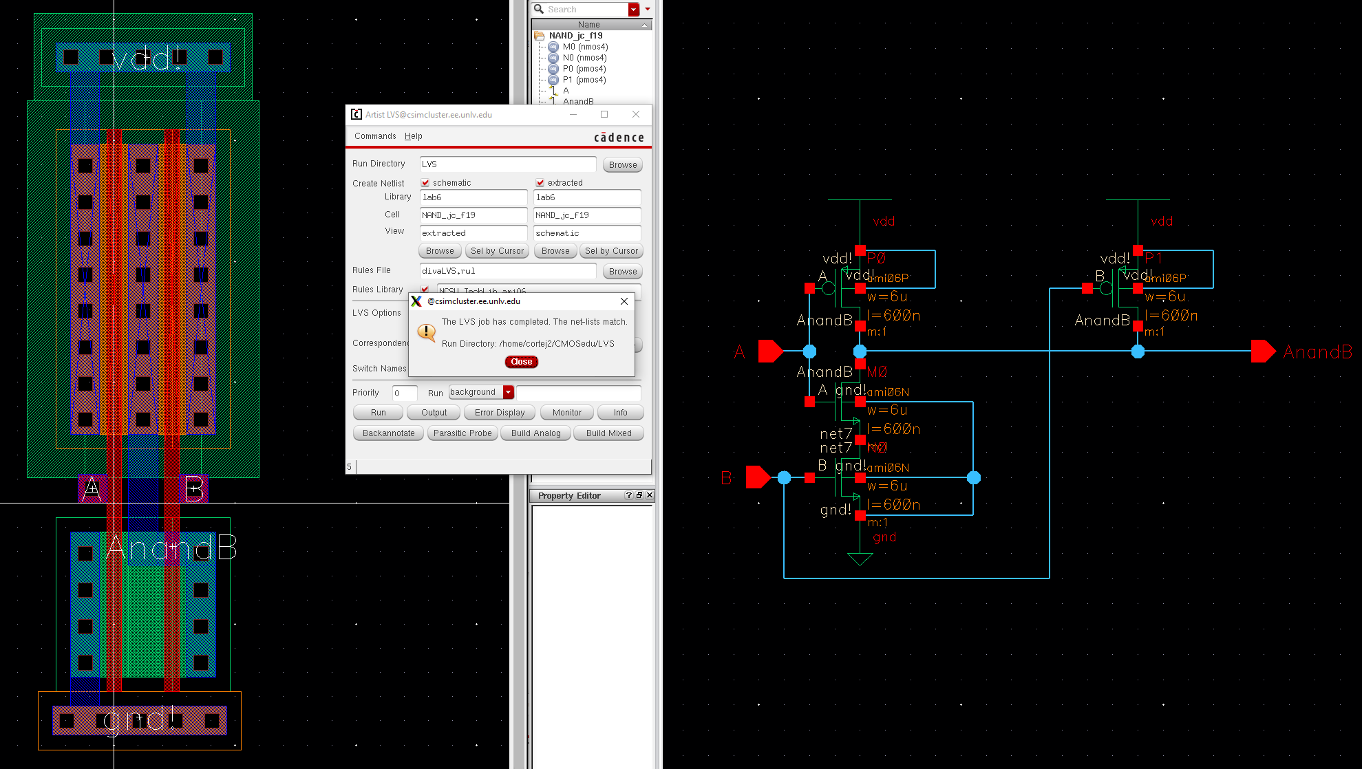 |
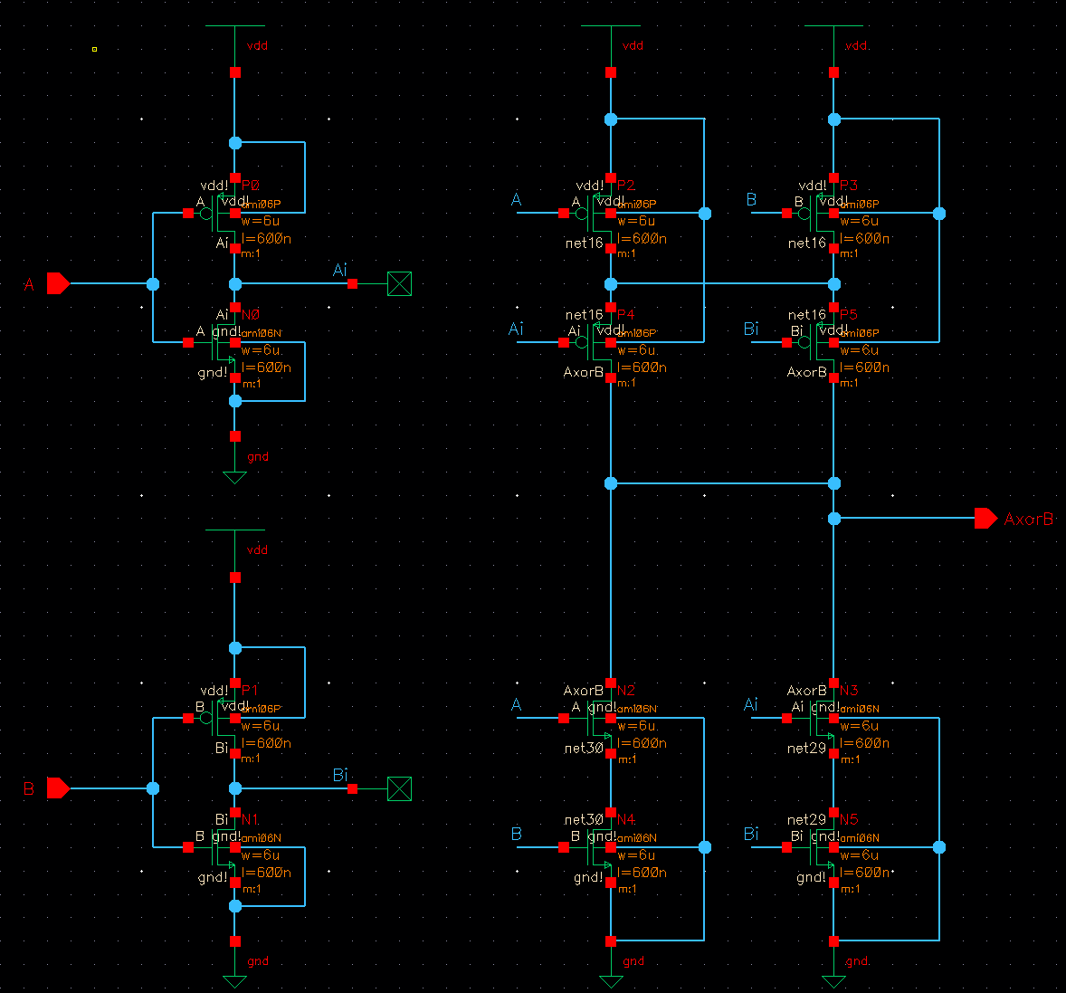
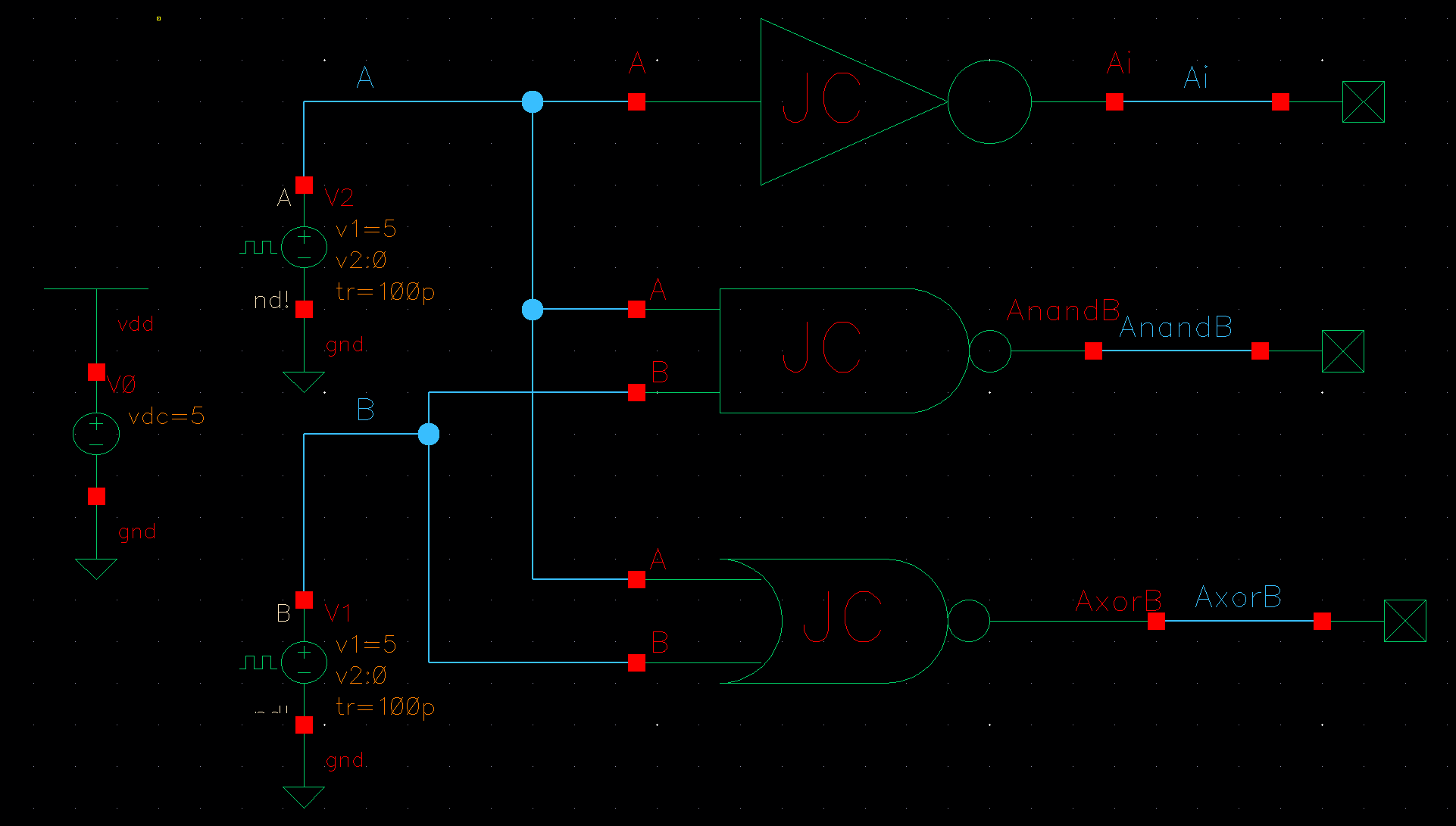
Below is the cell name, schematic, layout, DRC, symbol and LVS for the XOR gate.
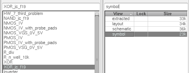
| XOR cell name | XOR schematic |
 |  |
| XOR layout | XOR symbol |
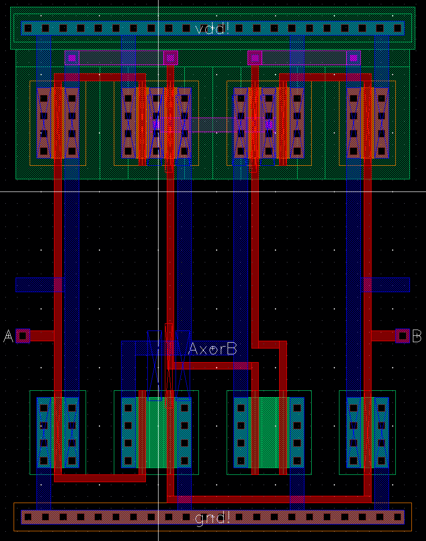 | 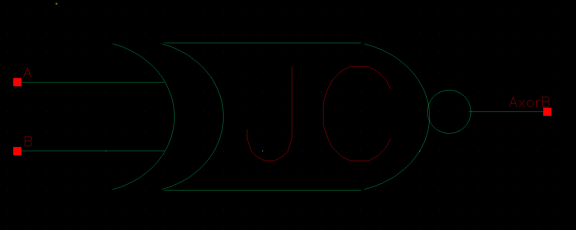 |
| XOR DRC | XOR LVS |
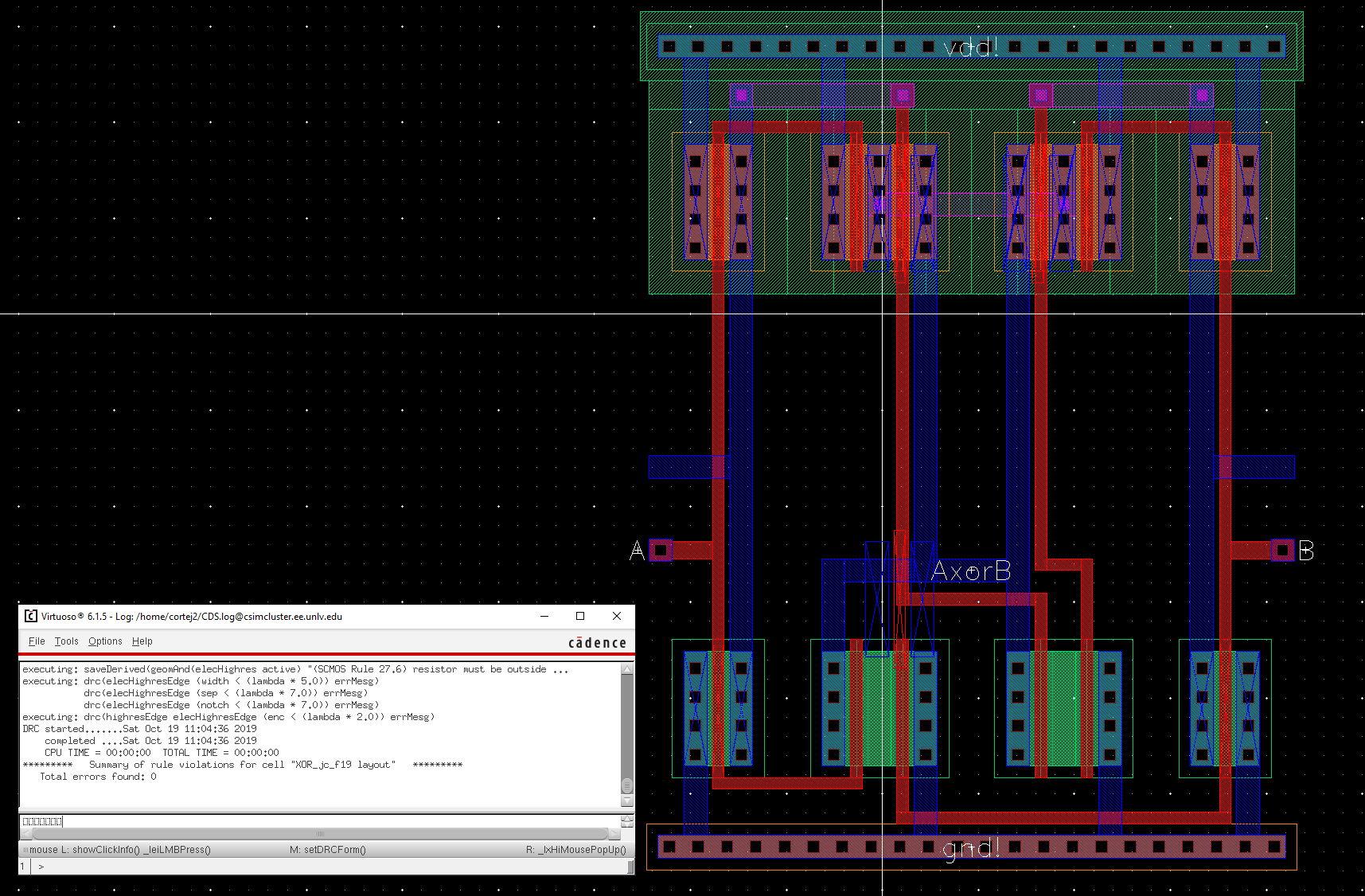 | 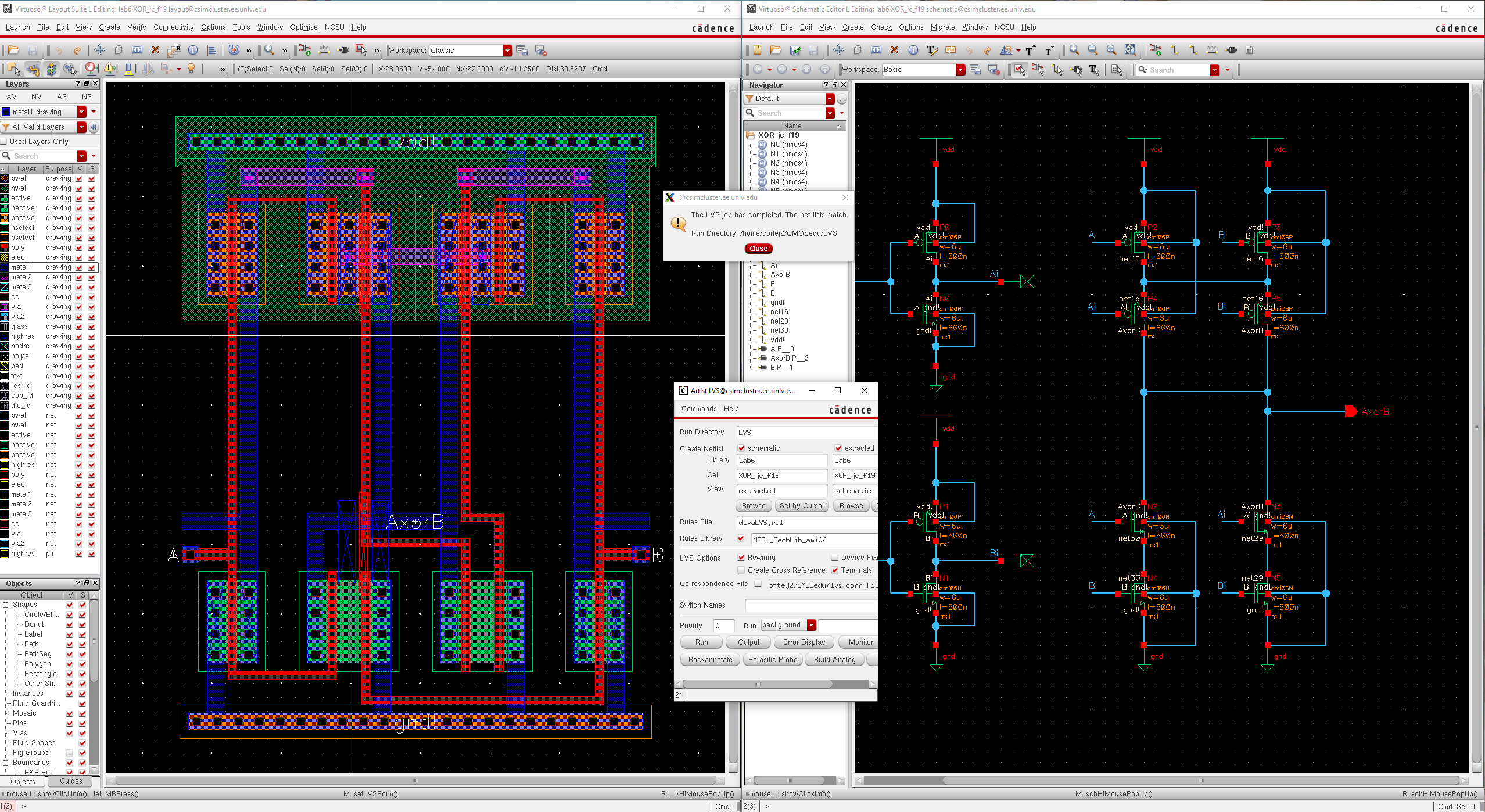 |
2) Creating a schematic to simulate the behavior of the gates to various inputs.
I then used Spectre to simulate the logical operation of the gates for all 4 possible inputs (00,01,10,11)
The results for the NAND and XOR are as what they should be. Ai is the inverted results of A
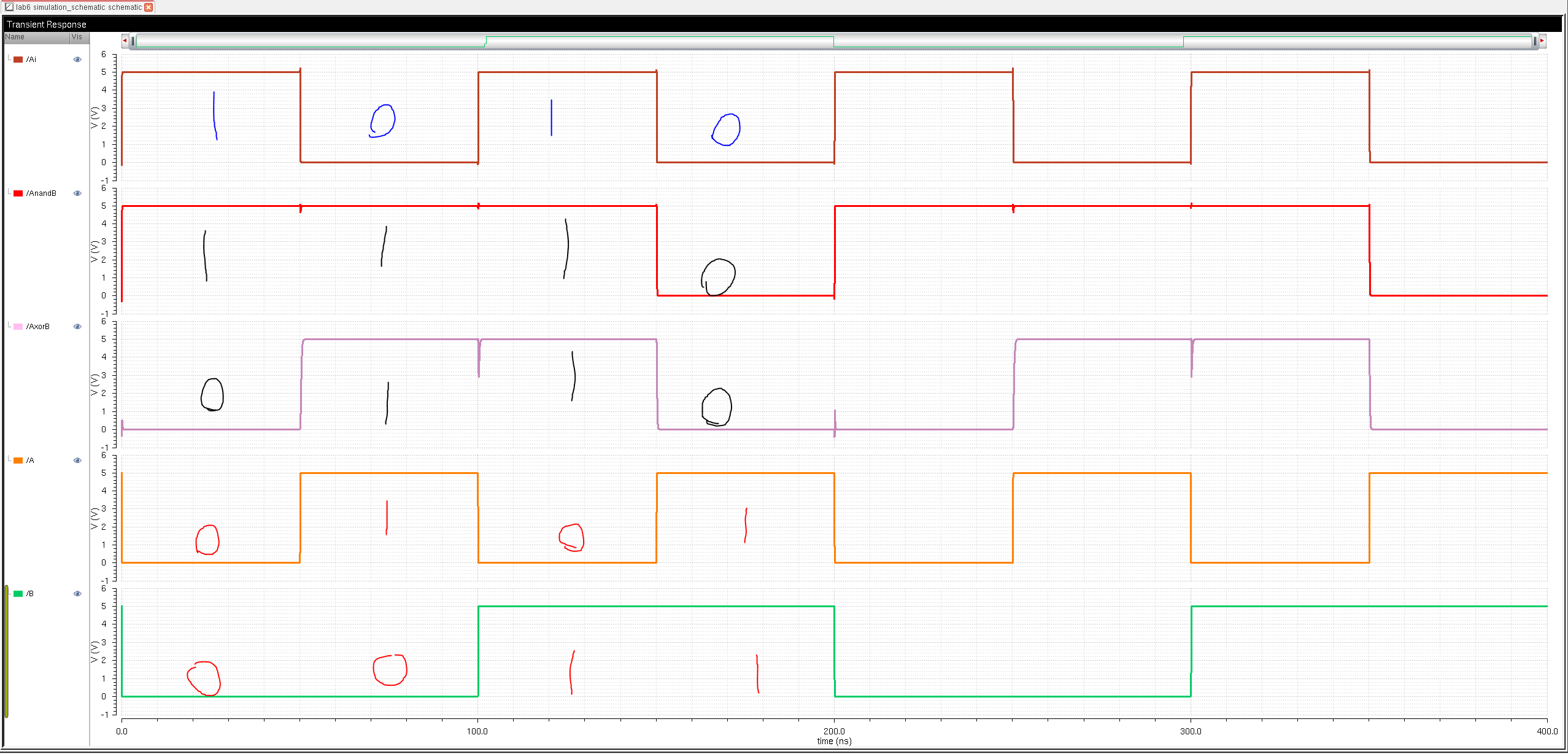
The timing input pulses cause glitches at the rising/falling edges. The gates react when there is a change in input. If there are two gates connected to each other, the first gate must output a proper signal before the second gate can produce the correct signal. This does not happen instantly since there is some time between rising/falling edges. Due to the time between rising and falling edges, there will be glitches where the proper response is not outputted immediately.
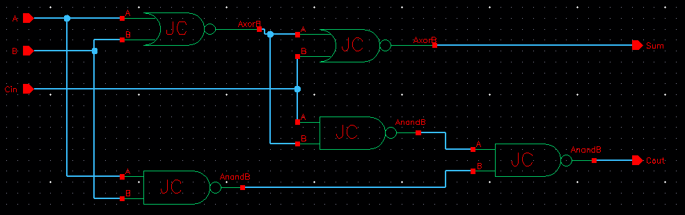
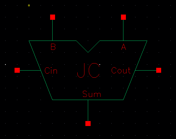
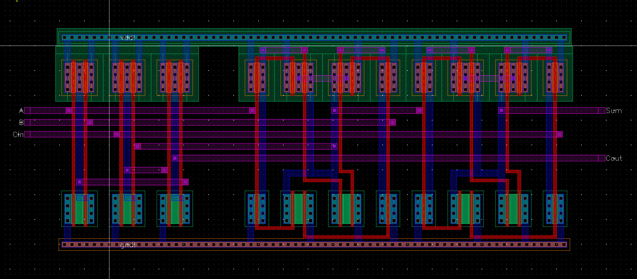
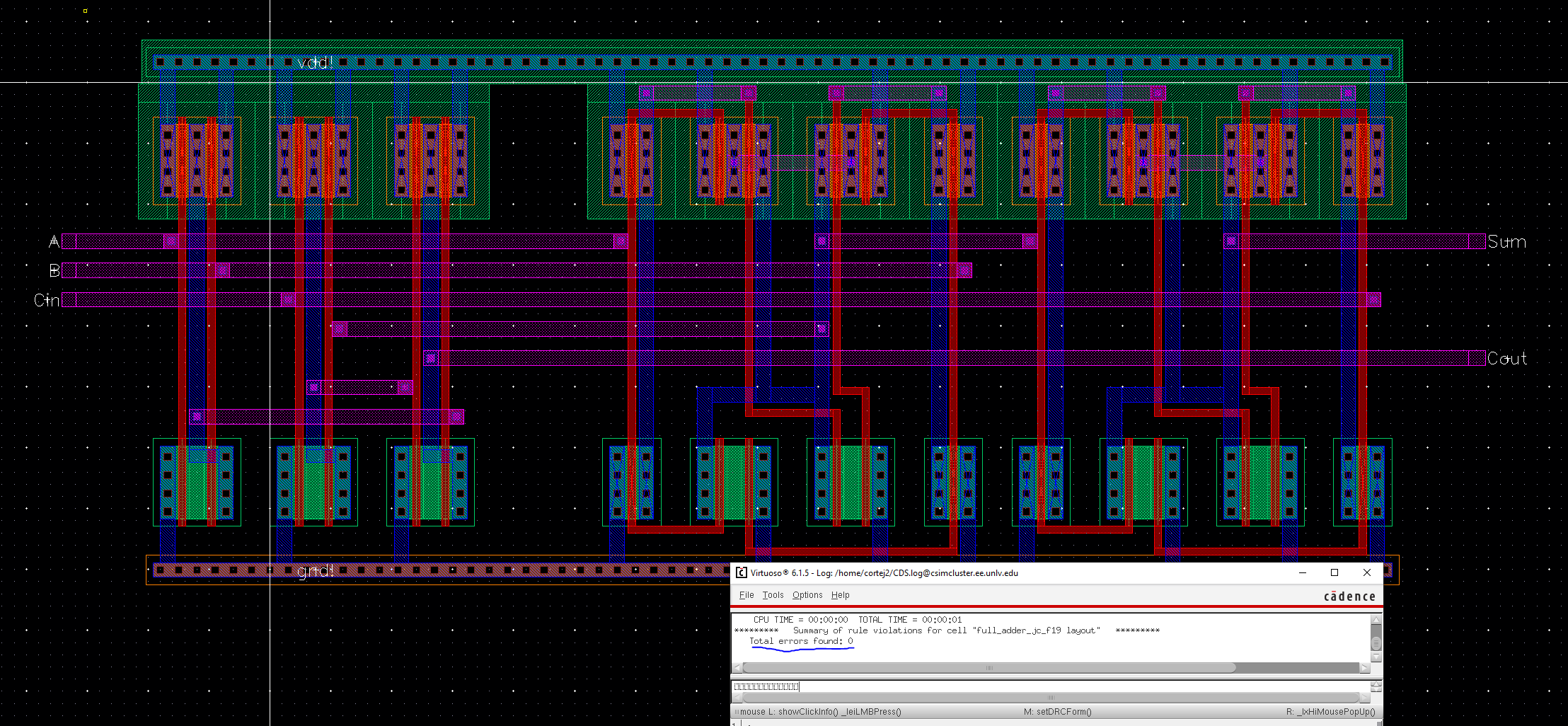
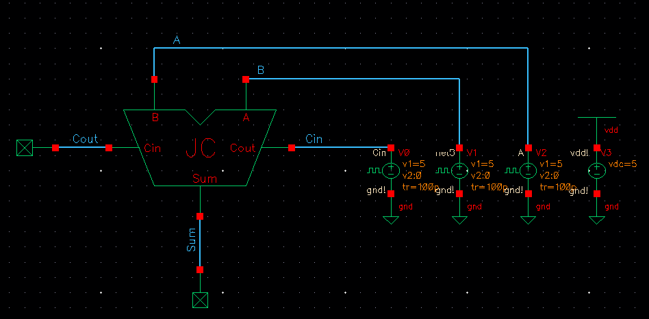
3) Creating the full adder
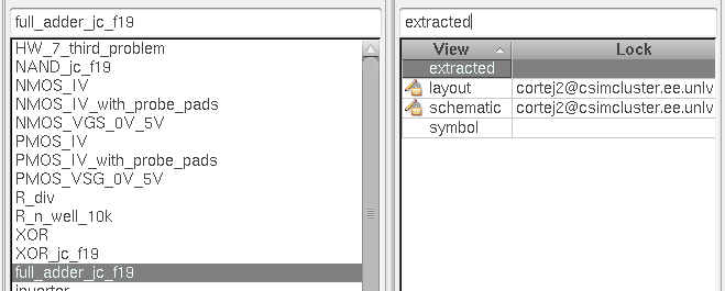
Below is the cell name, schematic, symbol, layout, and proof of DRC of the full adder.
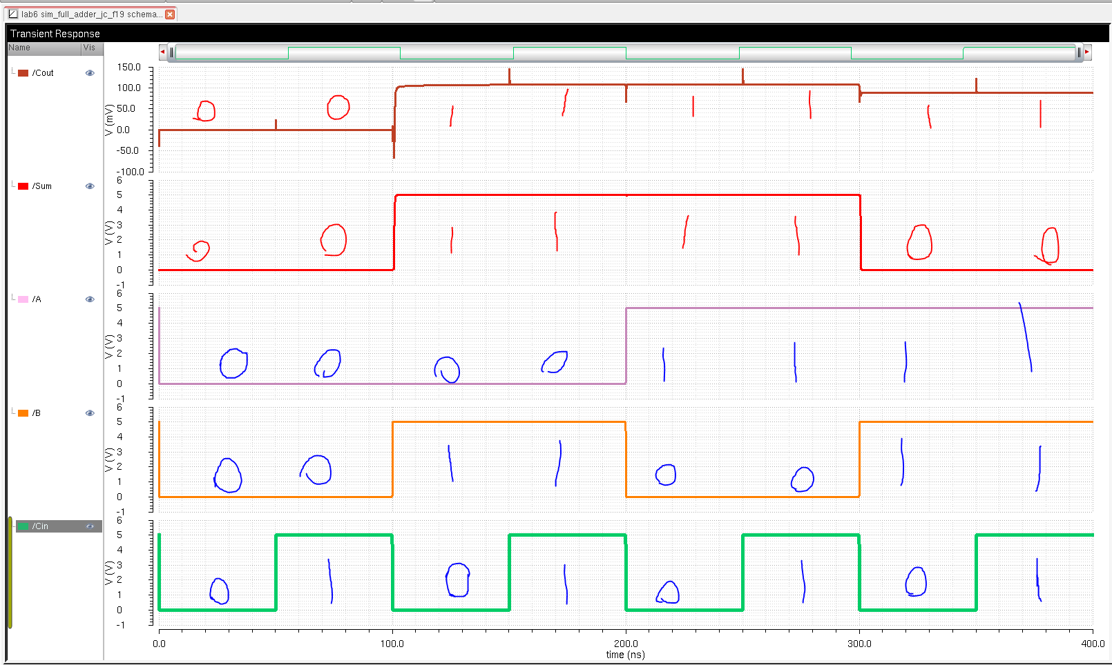
I then simulated the full adder schematic, below are the results
------------------------------------------------------------------------------------------------------------------------------------------------------------------------------------------------------------------------------------------
The link to the zip file with the folders used in this lab are linked here.